

Deep Tech Startups & Venture Capital: An Analysis of 2025 | Chapter 3
The annual report on the Deep Tech Cycle — 2025 in Themes: where value pools across semiconductors, quantum, and industrial materials.

Deep tech startups turn hard science into hard power: energy, materials, defense, health, and much more.
The real story is in wafers, tailings, turbines, data centers, advanced materials, and drill bits.
What follows is a deep dive to follow and understand the power of deep tech unleashed in 2025—and to be ready for 2026.

Greetings!
Welcome back to The Scenarionist’s annual Deep Tech Startups & Venture Capital report, which retraces the deep tech landscape of 2025.
It was a year when big promises had to pass a simple test: could they survive contact with supply chains, interest rates, and real industrial demand?
We have now reached Chapter 3 of this journey.
In Chapters 1 and 2, we followed deep tech “in data,” treating 2025 as a timeline.


Month after month, we looked at the tape: fundraises and down-rounds, new facilities and delayed ones, policy moves that unlocked projects and others that stalled them. Some numbers marked genuine breakthroughs; others simply showed where enthusiasm got ahead of fundamentals. Together, those chapters built a factual record of the year—useful to return to whenever the story starts to drift away from what actually happened.
In this chapter, the deep tech cycle is revisited through themes and sectors, and we look at where durable advantages, bottlenecks, and control points began to show themselves.
Enjoy the read!
– The Scenarionist Team
1. Semiconductors, Photonics & High-Speed Interconnect
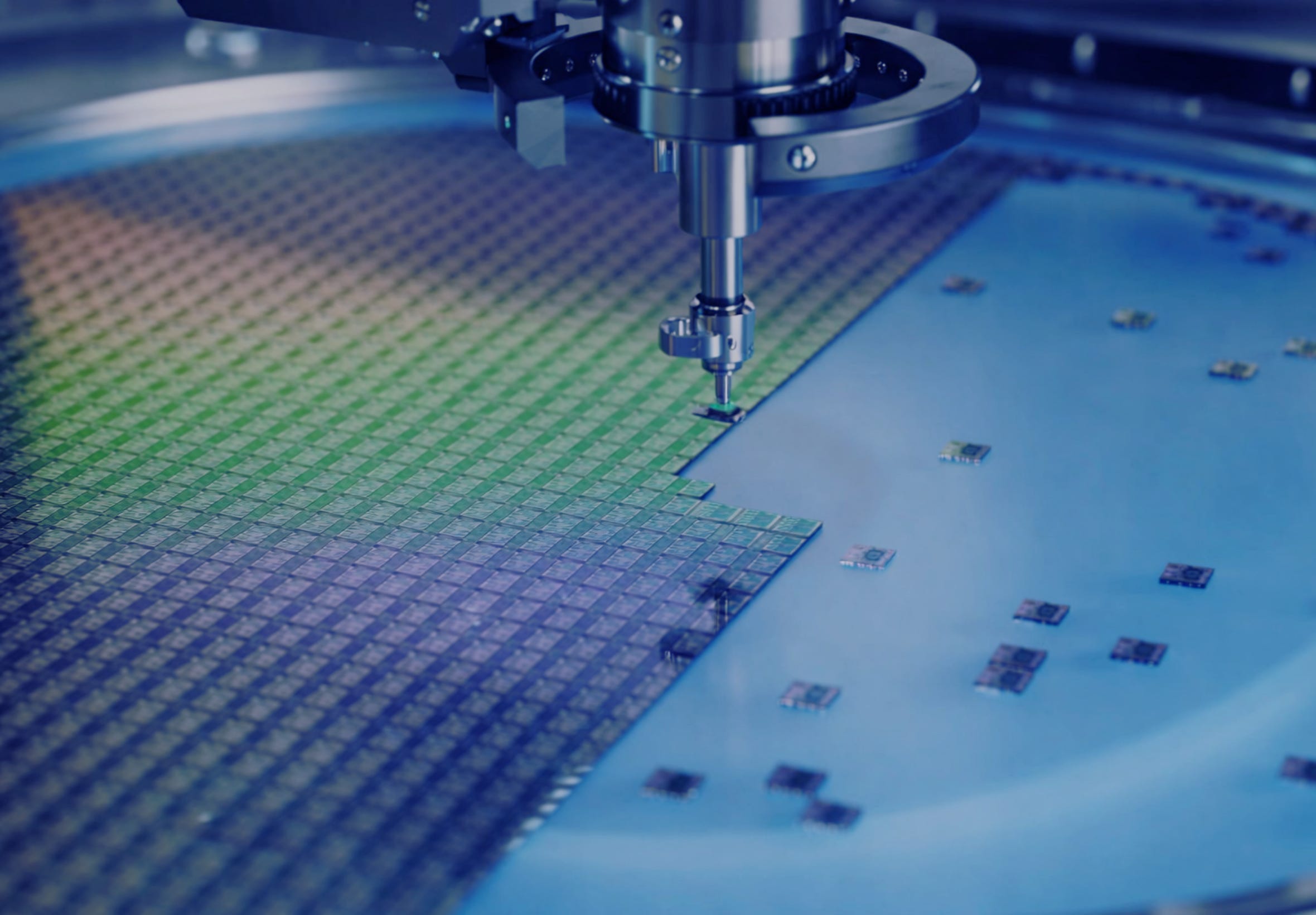
In semiconductors, photonics, and high-speed interconnect, 2025 made one point very clear: the AI bottleneck is no longer “how many chips,” but how fast bits move and how much rack-level physics can be controlled. Optical links and chiplet fabrics moved from research talks into corporate balance sheets. Specialized accelerators and secure architectures tried to lock in narrow but durable control points. Governments stepped in not only with grants, but with equity stakes in critical tools.
Throughout the year, a few questions kept repeating: where does value really pool when data movement—not raw FLOPs—is the constraint? Which semiconductor businesses can scale like infrastructure rather than like components? And how should founders and investors think about exits—IPO, strategic M&A, and now state-backed equity—around those bottlenecks?
1.1 The AI bottleneck moves to the physical layer
The clearest signal that interconnect, not compute, was setting the pace came from silicon photonics M&A.
In the U.S., Ciena’s acquisition of Nubis Communications for $270 million in cash crystallized a thesis that had been building for several quarters: inside the data center, the problem is now physical. Compute kept scaling; lanes between chips and racks did not.
Nubis brought co- and near-packaged optics advertising up to 6.4 Tb/s full-duplex per module, plus analog active copper links at 200 Gb/s per lane over four meters—exactly the range where AI clusters struggle with bandwidth and power budgets. The deal adds 50+ engineers and folds Nubis into Ciena’s high-speed SerDes roadmap, turning a traditional networking vendor into an owner of the optical engines themselves.
Inside the ecosystem, this was treated as the first meaningful silicon-photonics exit of the GenAI era and as a control move at a chokepoint—not as a speculative bet on fringe tech. The price reflects IP and talent at the precise point where AI training and inference fabrics hit copper limits.
A few months later, Marvell’s acquisition of Celestial AI pushed the same logic further.
Marvell had just sold its Automotive Ethernet business to Infineon for $2.5 billion in cash, then rotated that capital directly into Celestial AI’s Photonic Fabric. The deal was structured at $3.25 billion upfront, with a potential earn-out bringing the total to $5.5 billion. Celestial’s platform is designed to knit GPUs, other accelerators, and disaggregated memory into a single high-bandwidth optical fabric inside the data center. Marvell entered the deal from a position of strength—37% year-on-year revenue growth and 38% data-center revenue growth—but the portfolio rotation is the real story. It intentionally trades a solid, lower-leverage automotive unit for a position at what Marvell sees as the most acute AI bottleneck: moving data between chips, memory, and racks at lower energy per bit. Hyperscaler alignment reinforced this: AWS backed the deal with volume commitments and warrants, helping make a large, emerging TAM bankable.
In the same window, AMD’s acquisition of silicon-photonics specialist Enosemi underscored the same structural shift from “more FLOPs” to “fewer joules per bit.” Enosemi develops silicon-photonics circuits for co-packaged optics—targeting exactly the links that now limit delivered performance. The deal is about securing control over optical I/O around compute dies, not just adding another die.
Alongside these headline moves, a new crop of startups began raising capital around high-density, low-power architectures aimed at “breaking the AI power wall” in domains where packaging, interconnect, and power topology matter as much as transistor counts.
Taken together, these deals tell founders and investors that the physical layer—optics, packaging, interconnect, and power delivery—is now where strategic differentiation and M&A appetite concentrate. A photonics startup with credible co-packaged optics or analog I/O is no longer a curiosity; it is a potential answer to a line item in a hyperscaler’s capex plan.
1.2 Specialized AI silicon finds its footing—and its limits
While photonics grabbed headlines, 2025 also showed specialized AI silicon moving from slides to concrete milestones—revealing both where it works and where it struggles.
On the positive side, Encharge AI demonstrated what a tightly focused architecture looks like when it is tuned to a specific bottleneck. The company launched its EN100 accelerator, an analog-in-memory device optimized for high-throughput inference rather than training. It combines analog compute with compression logic to deliver more inference per watt and per rack unit, targeting both cloud and edge deployments where thermal budgets are tight and GPU-based inference starts to look expensive.
The pitch is not “highest TOPS.” It is “right architecture for the workload.” Large-scale inference is about serving many models at predictable latency inside a fixed power envelope. Encharge treats inference as infrastructure, not as an afterthought to training.
Elsewhere in the stack, Lowtek advanced a different thesis: that security can be enforced at the silicon level. Its memory-safe architecture aims to remove entire classes of software vulnerabilities by design, rather than relying on endless patching and monitoring. As autonomous systems enter vehicles, factories, and other safety-critical environments, this becomes a potential regulatory and contractual gate—moving part of the compliance burden down into hardware design.
The market also reminded everyone that not every architecture clears the bar. Rain AI—a neuromorphic chip startup backed by Sam Altman—reportedly explored a sale after a fundraising attempt fell through. The lesson is less about ambition and more about timing and ecosystem maturity: without a software stack and confident buyers, “new stack” hardware bets get repriced quickly.
Europe showed it is very much in the game. Belgium’s Vertical Compute raised an all-equity €20m seed to attack the AI “memory bottleneck,” positioning its approach around bringing memory physically closer to compute to reduce data-movement distances. The company explicitly targets the “memory wall” that is increasingly binding modern AI workloads.
And in the background, PowerLattice looked more like a power-delivery play than a pure compute reboot. Emerging from stealth with a $25m Series A in late 2025, it claimed a power-delivery chiplet that brings power closer to the processor package, cutting total compute power needs by more than 50%.
For builders and backers, the 2025 tape in specialized silicon reads less like a gold rush and more like a set of filters. Architectures tightly coupled to real bottlenecks—memory, security, inference economics, power delivery—attracted capital and partners. Designs that required a wholesale ecosystem leap without a clear bridge had a much harder time closing the next round.
1.3 Packaging, chiplets, and Europe’s interconnect ambitions
By 2025, the constraint was clearly not only on-die; it was in how dies talk to each other. That is where chiplets and advanced packaging stepped forward, and where Europe began to define its role.
Eliyan, a Santa Clara–born startup, chose Eindhoven’s High Tech Campus for a new R&D design center, placing itself in the middle of the ASML- and NXP-centric ecosystem. Eliyan develops die-to-die interconnects for chiplet architectures, claiming up to 4× performance at half the energy compared with alternatives. The target use case is familiar: AI accelerators constrained by memory bandwidth and package-level I/O rather than by their core compute units.
Strategically, this moves European leverage from the wafer to the package and system level, where much of the future value will accrue as UCIe-class standards mature. For Eliyan, proximity to advanced packaging providers and research institutes creates a testbed to prove that its gains hold across foundries and OSATs, not just in controlled demos.
At a deeper layer of the stack, xLight showed how far governments are willing to go to secure these building blocks. In late 2025, the U.S. Department of Commerce and NIST signed a letter of intent to inject up to $150 million into the semiconductor startup in exchange for an equity stake that could make the U.S. government its largest shareholder. Led by a former Intel CEO, xLight aims to bolt utility-scale free-electron lasers onto EUV lithography tools, sharpening the most delicate step in advanced chipmaking and pushing toward 2-nanometer features and higher wafer throughput.
This is not a classic grant; it is an explicit balance-sheet position in a pivotal part of the tool chain. For private capital, the logic is that the riskiest physics—laser-based EUV sources—are partly socialized, making it easier to finance surrounding ecosystems in metrology, optics, cooling, and power. The trade-off is that the state becomes a senior partner whose objectives are not purely financial. For adjacent businesses, that changes both risk and opportunity.
1.4 Photonics at the edge and in free space
Not all photonics stories in 2025 were about rack-scale fabrics. Several played out at the edge, where beam steering and optical control determine how autonomous systems and satellites see and communicate.
Lumotive raised $45 million in Series B funding to scale adoption of its Light-Control Metasurface (LCM™) chips, which provide solid-state optical beam steering without moving parts. Traditional mechanical systems in LiDAR and free-space optics struggle with speed, robustness, and cost. Lumotive’s LCM chips aim to replace that with programmable beam control, opening applications in AI-driven data-center optics, automotive and industrial LiDAR, and satellite communications—anywhere fast, precise steering of light is needed without complex mechanics.
The pattern matches the rest of the chapter: optical components are being re-cast as semiconductors. Once beam steering lives on a chip, it can follow the same scaling logic as other semis: high-volume manufacturing, tight integration, and predictable roadmaps. For autonomous mobility and satellite links, that can mean lower system cost and more flexible architectures. For hyperscale compute, it points toward a future where free-space optics and rack-level photonics share a design and supply base.
In parallel, quantum and classical photonics continued to converge at the application edge, as quantum-focused companies moved more photonics-based systems out of the lab and into early field deployments. Companies like SEEQC raised $30 million to develop chip-based, full-stack quantum computing platforms aimed at applications ranging from optimization and cryptography to AI modeling and secure communications.
For this chapter, the point is not to pre-empt the quantum discussion, but to note that techniques developed for quantum—low-loss photonics, precise timing, cryo-compatible control—are feeding back into mainstream interconnect and sensing. The same foundries and packaging lines that learn to handle quantum-grade materials and layouts can later serve very high-performance optical interconnect and signal-processing components.
1.5 Capital markets, exits, and new playbooks
Finally, 2025 also clarified a key question: what do exits look like for semiconductor and interconnect companies that sit close to AI infrastructure but are not themselves hyperscalers?
One answer came from public markets.
Blaize, an AI‑chip specialist, became the first AI‑hardware startup to go public in 2025, positioning itself as a provider of AI‑optimized processors rather than a generic fabless designer.
The SPAC-led listing signaled that public investors are willing to underwrite bespoke hardware for AI when the story is grounded in clear use cases and realistic scaling plans. For other chip companies, it reframes IPOs—whether traditional or SPAC-style—as a viable alternative to endless late-stage private rounds
Strategic M&A provided a second template. The Nubis–Ciena and Celestial AI–Marvell deals showed how incumbents now treat optical interconnect and photonics as core to their future revenue mix, not optional sidelines. Valuations are underwritten not by abstract TAM slides, but by direct mapping to AI data-center builds and measurable gains in watts per gigabit enabled by Nubis’ CPO/NPO engines and Celestial AI’s Photonic Fabric.
A third pattern appeared at the interface of hyperscalers and custom silicon. Meta’s acquisition of RISC‑V startup Rivos, fits a “buy the roadmap” strategy: securing RISC‑V talent and IP to accelerate in‑house AI accelerators and reduce dependency on external GPU suppliers.
Reported alongside Meta’s multibillion‑dollar GPU purchases and AI infrastructure commitments, it suggests a dual track—buy GPU capacity for the near term, build custom silicon to improve long‑term unit economics and strategic control.
At the edge of traditional capital markets, the xLight structure added a fourth pattern: the state as a cap-table participant in a single, highly specialized semiconductor company.
Equity stakes by governments—starting with laser-enabled lithography, but likely extending to other chokepoints—reshape how risk is shared and how private capital participates. They also bring in a new class of partner with time horizons and objectives that differ from both venture funds and corporate strategics.
Across 2025, the semiconductor, photonics, and interconnect tape pushed deep tech toward more concrete questions.
Exactly where in the stack does control over data movement translate into pricing power? When does it make sense to build a focused standalone architecture, and when is it better to aim for tight integration into someone else’s fabric? And how should builders and backers price an ecosystem where exits may come as IPOs, portfolio rotations, or government equity in companies treated as national infrastructure?
2. Advanced Materials & Industrial Chemistry

In 2025, advanced materials and industrial chemistry pivoted around a few clear shifts with real industrial and financial impact. Magnet-grade rare-earth recycling moved from pilots to serious capacity planning. Chemical recycling